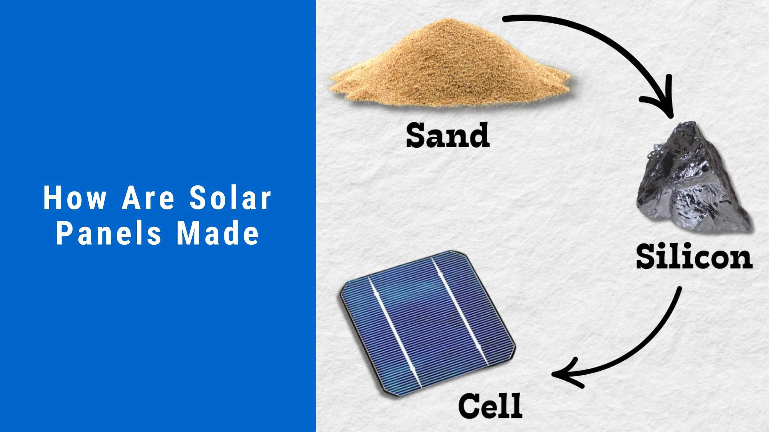
Solar panels are fascinating technology that converts sunlight into electricity with reasonable efficiency. But do you ever wonder how they are made? It all begins with something as innocuous as sand. Let’s walk through the entire journey, from raw materials to the final solar panel.
1. It All Begins with Sand
Silicon — the material that forms the base of nearly all solar panel technologies comes from silica sand (SiO₂). Silicon is the second most common element in the Earth’s crust, so we aren’t going to run out of it anytime soon! However, the kind of sand used to make those cells must be very pure to be used in creating high-efficiency solar panels.
Extracting Silicon from Sand
Silicon is extracted from silica sand by heating it in a high-temperature furnace (approximately 2000°C) with carbon-rich material such as coal, charcoal, coke, or wood chips. This reaction reduces the silicon dioxide (SiO₂) and produces metallurgical-grade silicon (MG-Si) at 99.99% purity.
The Chemical Reaction:
SiO₂ (sand) + C (carbon source) ⇾ Si (silicon) + CO₂ (carbon dioxide)This process employs an electric arc furnace in which an electric current melts the mixture, breaking the bonds between silicon and oxygen. Once cooled, the resulting silicon forms shiny, metallic crystals.
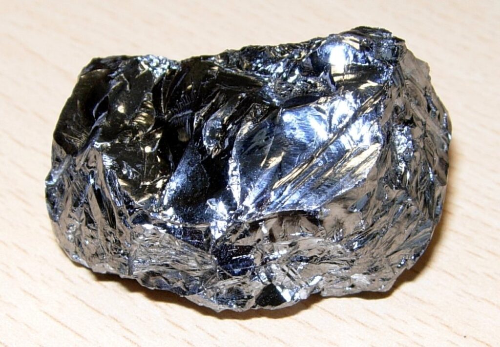
MG-Si is already fairly pure, but for solar panels, you need ultra-pure silicon, 99.999999% pure silicon, aka 9N purity.
2. Refining Silicon: Turning Sand into Solar-Grade Silicon
+ The Siemens Method for Producing Polysilicon
MG-Si goes through a purification procedure called the Siemens process to achieve the 9N purity level. This is how it operates:
At 300°C, MG-Si and hydrogen chloride (HCl) react to produce the volatile compound trichlorosilane (SiHCl₃).
To get rid of contaminants, the trichlorosilane gas is distilled several times.
Ultra-pure polysilicon is created when the purified gas is finally broken down at high temperatures on a heated silicon rod.
The Reactions of Chemicals:
Si (MG-Si) + 3HCl → SiHCl₃ (trichlorosilane) + H₂ SiHCl₃ → Si (pure polysilicon) + Cl₂The result of this process is polysilicon, which appears in the picture below as big, shiny, and brittle chunks.
The purified silicon can now proceed in one of two ways: producing either monocrystalline or polycrystalline solar cells.
3A. Polycrystalline Silicon Process
Polycrystalline cells were more widely used in the past. You may have noticed older solar panels with a noticeable blue tint; these were polycrystalline panels. They are becoming less common because of their lower efficiency compared to monocrystalline cells, though some manufacturers still make them.
The casting process involves pouring melted silicon into square molds that contain boron impurities and letting them cool.
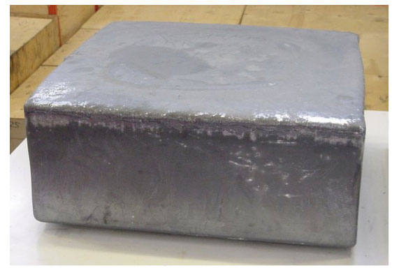
- Cutting into Wafers: The thin wafers, about 200 microns, are cut from the solid silicon blocks.
- Doping and Surface Treatment: A PN junction will be created by treating the surface and depositing a layer of phosphorus impurities.
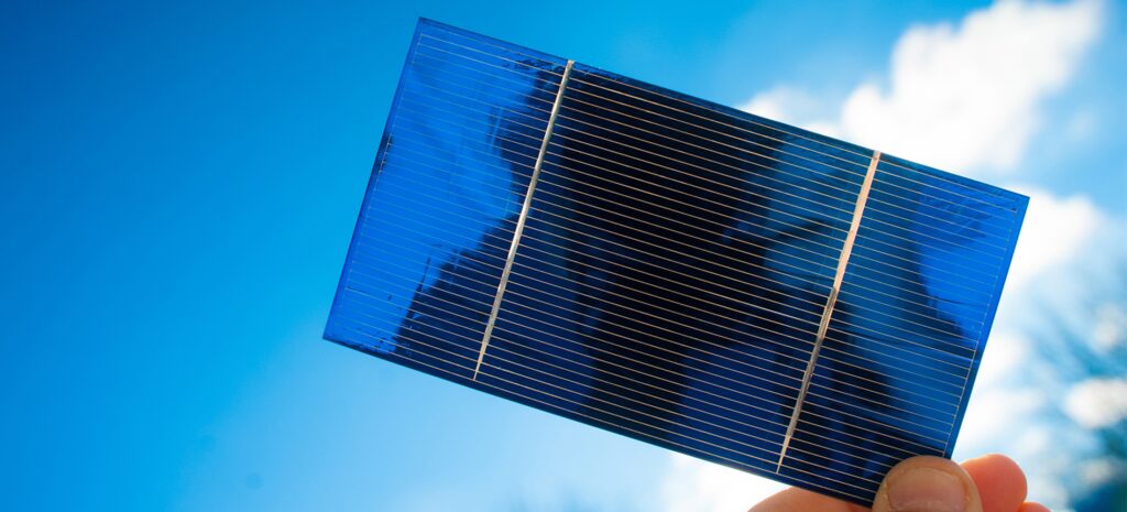
Polycrystalline panels are popular for installations on a tight budget because they are more economical despite having slightly lower efficiency.
3B. Monocrystalline Silicon Process
Higher efficiency is possible because monocrystalline solar cells are composed of a single crystal structure. This is how they are produced:
- The Czochralski Method: A pure seed crystal is dipped in melted silicon and slowly rotated upward. As a result, a sizable, single-crystal silicon ingot is produced.
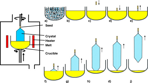
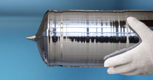
- Cutting into Wafers: A diamond wire saw is used to cut the cylindrical ingot into thin wafers.
- Doping and Etching: Phosphorus or boron is applied to the wafers to form a semiconductor junction.
Although monocrystalline panels are more costly to manufacture, they are more efficient. These days, they control the market, and black monocrystalline panels are found in most new installations.
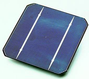
4. Solar Cell Assembly: Turning Wafers into Power Generators
After silicon wafers are obtained, they must be processed to create working solar cells:
- Texturing: To enhance light absorption and lessen reflection, the wafer surface is textured.
- Anti-Reflective Coating: To improve light capture, a unique coating is applied.
- Metal Contacts: To conduct the electricity the cell produces, thin metal lines are added.
5. Assembling the Solar Panel
Putting everything together to create a functional solar panel is the last step:
- Cell Connection: Solar cells are connected in parallel or series to obtain the required voltage and current.
- Lamination: EVA (ethylene vinyl acetate) is used to laminate the cells to keep them in place.
- Glass and Frame: For durability, an aluminum frame is added, and a protective glass sheet is placed on top.
- Installation of the Junction Box: A junction box at the rear connects the electrical output.
- Quality Testing: To guarantee performance and longevity, every panel undergoes a rigorous testing process that includes electroluminescence (EL) imaging and flash testing.
6. The Finished Product: Ready to Capture the Sun!
Once they have passed all tests, the solar panels are packaged and sent to residences, companies, and solar farms worldwide. After installation, they can produce clean, renewable energy for over 25 years!
It’s incredible how something as ordinary as sand can be turned into the sophisticated solar panels that run our entire planet. The process combines engineering, chemistry, and physics, from silicon extraction to solar cell production and panel assembly.
Remember this the next time you see a solar panel: it was once sand.
Frequently Asked Questions (FAQs)
Are solar cells made from sand?
Yes, silicon-based solar cells are made from sand—but not just any sand. It’s refined quartz sand processed into high-purity silicon.
Can we make a solar cell at home?
It’s possible on a very basic level, but solar cells need high-tech equipment and materials unavailable at home.
What is the best sand for solar cells?
High-purity quartz sand is the best. It contains silicon dioxide (SiO₂), which is refined into solar-grade silicon.
How is sand turned into a solar cell?
The sand is processed into pure silicon, which is then made into wafers, treated with special coatings, and assembled into solar cells.
Why is silicon used in solar cells?
Silicon is abundant, durable, and has excellent properties to convert sunlight into electricity efficiently.
Can we use beach sand to make solar cells?
No, beach sand contains impurities and isn’t pure enough. Only specific quartz-rich sand is suitable.
Are all solar panels made from sand?
Not all. While most are silicon-based (made from sand), some advanced types use other materials like perovskite or thin films.


